Springer Series in Materials Science
3 primary works
Book 116
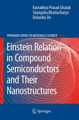
Einstein Relation in Compound Semiconductors and Their Nanostructures
by Kamakhya Prasad Ghatak, Sitangshu Bhattacharya, and Debashis De
Published 20 November 2008
In recent years, with the advent of ?ne line lithographical methods, molecular beam epitaxy, organometallic vapour phase epitaxy and other experimental techniques, low dimensional structures having quantum con?nement in one, two and three dimensions (such as inversion layers, ultrathin ?lms, nipi's, quantum well superlattices, quantum wires, quantum wire superlattices, and quantum dots together with quantum con?ned structures aided by various other ?elds) have attracted much attention, not only for their potential in uncovering new phenomena in nanoscience, but also for their interesting applications in the realm of quantum e?ect devices. In ultrathin ?lms, due to the reduction of symmetry in the wave-vector space, the motion of the carriers in the direction normal to the ?lm becomes quantized leading to the quantum size e?ect. Such systems ?nd extensive applications in quantum well lasers, ?eld e?ect transistors, high speed digital networks and also in other low dimensional systems. In quantum wires, the carriers are quantized in two transverse directions and only one-dimensional motion of the carriers is allowed.
The transport properties of charge carriers in quantum wires, which may be studied by utilizing the similarities with optical and microwave waveguides, are currently being investigated. Knowledge regarding these quantized structures may be gained from original research contributions in scienti?c journals, proceedings of international conferences and various - view articles.
The transport properties of charge carriers in quantum wires, which may be studied by utilizing the similarities with optical and microwave waveguides, are currently being investigated. Knowledge regarding these quantized structures may be gained from original research contributions in scienti?c journals, proceedings of international conferences and various - view articles.
Book 137
Thermoelectric Power in Nanostructured Materials
by Kamakhya Prasad Ghatak and Sitangshu Bhattacharya
Published 31 July 2010
The merging of the concept of introduction of asymmetry of the wave vector space of the charge carriers in semiconductors with the modern techniques of fabric- ing nanostructured materials such as MBE, MOCVD, and FLL in one, two, and three dimensions (such as ultrathin ?lms, nipi structures, inversion and accumu- tion layers, quantum well superlattices, carbon nanotubes, quantum wires, quantum wire superlattices, quantumdots, magnetoinversionand accumulationlayers, qu- tum dot superlattices, etc. ) spawns not only useful quantum effect devices but also unearth new concepts in the realm of nanostructured materials science and related disciplines. It is worth remaking that these semiconductor nanostructures occupy a paramount position in the entire arena of low-dimensional science and technology by their own right and ?nd extensive applications in quantum registers, resonant tunneling diodes and transistors, quantum switches, quantum sensors, quantum logic gates, heterojunction ?eld-effect, quantum well and quantum wire trans- tors, high-speed digital networks, high-frequency microwave circuits, quantum cascade lasers, high-resolution terahertz spectroscopy, superlattice photo-oscillator, advanced integrated circuits, superlattice photocathodes, thermoelectric devices, superlattice coolers, thin ?
lm transistors, intermediate-band solar cells, micro- tical systems, high-performanceinfrared imaging systems, bandpass ?lters, thermal sensors, optical modulators, optical switching systems, single electron/molecule electronics, nanotube based diodes, and other nanoelectronic devices.
lm transistors, intermediate-band solar cells, micro- tical systems, high-performanceinfrared imaging systems, bandpass ?lters, thermal sensors, optical modulators, optical switching systems, single electron/molecule electronics, nanotube based diodes, and other nanoelectronic devices.
Book 167
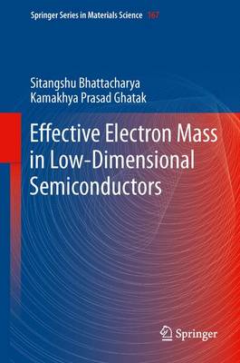
Effective Electron Mass in Low-Dimensional Semiconductors
by Sitangshu Bhattacharya and Kamakhya Prasad Ghatak
Published 6 October 2012
This book deals with the Effective Electron Mass (EEM) in low dimensional semiconductors. The materials considered are quantum confined non-linear optical, III-V, II-VI, GaP, Ge, PtSb2, zero-gap, stressed, Bismuth, carbon nanotubes, GaSb, IV-VI, Te, II-V, Bi2Te3, Sb, III-V, II-VI, IV-VI semiconductors and quantized III-V, II-VI, IV-VI and HgTe/CdTe superlattices with graded interfaces and effective mass superlattices. The presence of intense electric field and the light waves change the band structure of optoelectronic semiconductors in fundamental ways, which have also been incorporated in the study of the EEM in quantized structures of optoelectronic compounds that control the studies of the quantum effect devices under strong fields. The importance of measurement of band gap in optoelectronic materials under strong electric field and external photo excitation has also been discussed in this context. The influence of crossed electric and quantizing magnetic fields on the EEM and the EEM in heavily doped semiconductors and their nanostructures is discussed. This book contains 200 open research problems which form the integral part of the text and are useful for both Ph. D aspirants and researchers in the fields of solid-state sciences, materials science, nanoscience and technology and allied fields in addition to the graduate courses in modern semiconductor nanostructures.
The book is written for post graduate students, researchers and engineers, professionals in the fields of solid state sciences, materials science, nanoscience and technology, nanostructured materials and condensed matter physics.
The book is written for post graduate students, researchers and engineers, professionals in the fields of solid state sciences, materials science, nanoscience and technology, nanostructured materials and condensed matter physics.


