The Springer International Series in Engineering and Computer Science
21 primary works
Book 117
Low-Noise Wide-Band Amplifiers in Bipolar and CMOS Technologies
by Zhong Yuan Chong and Willy M.C. Sansen
Book 137
Symbolic Analysis for Automated Design of Analog Integrated Circuits
by Georges Gielen and Willy M.C. Sansen
Book 223
High-Performance CMOS Continuous-Time Filters
by Jose Silva-martinez, Michiel Steyaert, and Willy M.C. Sansen
The organization of this text is hierarchical, starting with the design consideration of the basic building blocks and ending with the design of several high-performance continuous-time filters. Most of the circuits have been fabricated, theoretically analyzed and simulated, and silicon measurement results are compared with each other.
High-Performance CMOS Continuous-Time Filters can be used as a text book for senior or graduate courses on this topic and can also be useful for industrial engineers as a reference book.
Book 225
Analog Interfaces for Digital Signal Processing Systems
by Frank op 't Eynde and Willy M.C. Sansen
Book 384
Analog VLSI Integration of Massive Parallel Signal Processing Systems
by Peter Kinget and Michiel Steyaert
Book 411
Book 451
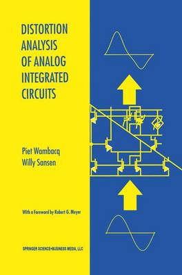
Distortion Analysis of Analog Integrated Circuits
by Piet Wambacq and Willy M.C. Sansen
Book 493
Design of Low-Voltage Low-Power CMOS Delta-Sigma A/D Converters
by Vincenzo Peluso, Michiel Steyaert, and Willy M.C. Sansen
A method of implementing the classic single loop and cascaded Delta-Sigma modulator topologies with half delay integrators is presented. Those topologies are studied in order to find the parameters that maximise the performance in terms of peak SNR. Based on a linear model, the performance degradations of higher order single loop and cascaded modulators, compared to a hypothetical ideal modulator, are quantified.
An overview of low voltage Switched Capacitor design techniques, such as the use of voltage multipliers, low VtMOST devices and the Switched Opamp Technique, is given. An in-depth discussion of the present status of the Switched Opamp Technique covers the single-ended Original Switched Opamp Technique, the Modified Switched Opamp Technique, which allows lower supply voltage operation, and differential implementation including common mode control techniques.
The restrictions imposed on the analog circuits by low supply voltage operation are investigated. Several low voltage circuit building blocks, some of which are new, are discussed. A new low voltage class AB OTA, especially suited for differential Switched Opamp applications, together with a common mode feedback amplifier and a comparator are presented and analyzed.
As part of a systematic top-down design approach, the non-ideal charge transfer of the Switched Opamp integrator cell is modeled, based upon several models of the main opamp non-ideal characteristics. Behavioral simulations carried out with these models yield the required opamp specifications that ensure that the intended performance is met in an implementation.
A power consumption analysis is performed. The influence of all design parameters, especially the low power supply voltage, is highlighted. Design guidelines towards low power operation are distilled.
Two implementations are presented together with measurement results. The first one is a single-ended implementation of a Delta-Sigma ADC operating with 1.5V supply voltage and consuming 100 W for a 74 dB dynamic range in a 3.4 kHz bandwidth. The second implementation is differential and operates with 900 mV. It achieves 77 dB dynamic range in 16 kHz bandwidth and consumes 40 W.
Design of Low-Voltage Low-Power CMOS Delta-Sigma A/D Converters is essential reading for analog design engineers and researchers.
Book 501
Analog Layout Generation for Performance and Manufacturability
by Koen Lampaert, Georges Gielen, and Willy M.C. Sansen
In the past, automatic analog layout tools tried to optimize the layout without quantifying the performance degradation introduced by layout parasitics. Therefore, it was not guaranteed that the resulting layout met the specifications and one or more layout iterations could be needed. In Analog Layout Generation for Performance and Manufacturability, the authors propose a performance driven layout strategy to overcome this problem. In this methodology, the layout tools are driven by performance constraints, such that the final layout, with parasitic effects, still satisfies the specifications of the circuit. The performance degradation associated with an intermediate layout solution is evaluated at runtime using predetermined sensitivities. In contrast with other performance driven layout methodologies, the tools proposed in this book operate directly on the performance constraints, without an intermediate parasitic constraint generation step. This approach makes a complete and sensible trade-off between the different layout alternatives possible at runtime and therefore eliminates the possible feedback route between constraint derivation, placement and layout extraction.
Besides its influence on the performance, layout also has a profound impact on the yield and testability of an analog circuit. In Analog Layout Generation for Performance and Manufacturability, the authors outline a new criterion to quantify the detectability of a fault and combine this with a yield model to evaluate the testability of an integrated circuit layout. They then integrate this technique with their performance driven routing algorithm to produce layouts that have optimal manufacturability while still meeting their performance specifications.
Analog Layout Generation for Performance and Manufacturability will be of interest to analog engineers, researchers and students.
Book 661
CMOS Cellular Receiver Front-Ends: from Specification to Realization deals with the design of the receive path of a highly-integrated CMOS cellular transceiver for the GSM-1800 cellular system. The complete design trajectory is covered, starting from the documents describing the standard down to the systematic development of CMOS receiver ICs that comply to the standard. The design of CMOS receivers is tackled at all abstraction levels: from architecture level, via circuit level, down to the device level, and the other way around.
The theoretical core of the book discusses the fundamental and more advanced aspects of RF CMOS design. It focuses specifically on all aspects of the design of high-performance CMOS low-noise amplifiers.
Book 672
A Computer-Aided Design and Synthesis Environment for Analog Integrated Circuits
by Geert Van Der Plas, Georges Gielen, and Willy M.C. Sansen
This text addresses the design methodologies and CAD tools available for the systematic design and design automation of analogue integrated circuits. Two complementary approaches discussed increase analogue design productivity, demonstrated throughout using design times of the different design experiments undertaken.
Book 724
CMOS Fractional-N Synthesizers starts with a comprehensive introduction to general frequency synthesis. Different architectures and synthesizer building blocks are discussed with their relative importance on synthesizer specifications. The process of synthesizer specification derivation is illustrated with the DCS-1800 standard as a general test case.
The book tackles the design of fractional-N synthesizers in CMOS on circuit level as well as system level. The circuit level focuses on high-speed prescaler design up to 12 GHz in CMOS and on fully integrated, low-phase-noise LC-VCO design. High-Q inductor integration and simulation in CMOS is elaborated and flicker noise minimization techniques are presented, ranging from bias point choice to noise filtering techniques.
On a higher level, a systematic design strategy has been developed that trades off all noise contributions and fast dynamics for integrated capacitance (area). Moreover, a theoretical DeltaSigma phase noise analysis is presented, extended with a fast non-linear analysis method to accurately predict the influence of PLL non-linearities on the spectral purity of the DeltaSigma fractional-N frequency synthesizers.
Book 738
Systematic Design of Analog IP Blocks
by Jan Vandenbussche, Georges Gielen, and Michiel Steyaert
This book introduces a design methodology that can help to bridge the productivity gap. Two different types of designs, depending on the design challenge, have been identified. To validate the presented methodologies, the authors have selected and designed accordingly three different industrial-strength applications.
Book 747
This practical guide and introduction to the design of key RF building blocks used in high data rate transmitters emphasizes CMOS circuit techniques applicable to oscillators and upconvertors. The book is written in an easily accessible manner, without losing detail on the technical side.
Book 759
Design and Analysis of High Efficiency Line Drivers for Xdsl
by Tim Piessens and Michiel Steyaert
Design and Analysis of High Efficiency Line Drivers for xDSL covers the most important building block of an xDSL (ADSL, VDSL, ...) system: the line driver. Traditional Class AB line drivers consume more than 70% of the total power budget of state-of-the-art ADSL modems. This book describes the main difficulties in designing line drivers for xDSL. The most important specifications are elaborated staring from the main properties of the channel and the signal properties. The traditional (class AB), state-of-the-art (class G) and future technologies (class K) are discussed.
The main part of Design and Analysis of High Efficiency Line Drivers for xDSL describes the design of a novel architecture: the Self-Oscillating Power Amplifier or SOPA.
Book 761
Static and Dynamic Performance Limitations for High Speed D/A Converters
by Anne van den Bosch, Michiel Steyaert, and Willy M.C. Sansen
Starting from the definition of the basic specifications for a D/A converter, the elements determining the static and dynamic performance are identified. Different guidelines based on scientific derivations are suggested to optimize this performance. Furthermore, a new closed formula has been derived to account for the influence of the transistor mismatch on the achievable resolution of the current-steering D/A converter. To allow a thorough understanding of the dynamic behavior, a new factor has been introduced. Moreover, the frequency dependency of the output impedance introduces harmonic distortion components which can limit the maximum attainable spurious free dynamic range. Finally, the last part of the book gives an overview on different existing transistor mismatch models and the link with the static performance of the D/A converter.
Book 843
Lna-Esd Co-Design for Fully Integrated CMOS Wireless Receivers
by Paul Leroux, Michiel Steyaert, and LeRoux Paul
LNA-ESD Co-Design for Fully Integrated CMOS Wireless Receivers fits in the quest for complete CMOS integration of wireless receiver front-ends. With a combined discussion of both RF and ESD performance, it tackles one of the final obstacles on the road to CMOS integration. The book is conceived as a design guide for those actively involved in the design of CMOS wireless receivers.
The book starts with a comprehensive introduction to the performance requirements of low-noise amplifiers in wireless receivers. Several popular topologies are explained and compared with respect to future technology and frequency scaling. The ESD requirements are introduced and related to the state-of-the-art protection devices and circuits.
LNA-ESD Co-Design for Fully Integrated CMOS Wireless Receivers provides an extensive theoretical treatment of the performance of CMOS low-noise amplifiers in the presence of ESD-protection circuitry. The influence of the ESD-protection parasitics on noise figure, gain, linearity, and matching are investigated. Several RF-ESD co-design solutions are discussed allowing both high RF-performance and good ESD-immunity for frequencies up to and beyond 5 GHz. Special attention is also paid to the layout of both active and passive components.
LNA-ESD Co-Design for Fully Integrated CMOS Wireless Receivers offers the reader intuitive insight in the LNA's behavior, as well as the necessary mathematical background to optimize its performance. All material is experimentally verified with several CMOS implementations, among which a fully integrated GPS receiver front-end. The book is essential reading for RF design engineers and researchers in the field and is also suitable as a text book for an advanced course on the subject.Book 851
Matching Properties of Deep Sub-Micron Mos Transistors
by Jeroen A Croon, Willy Sansen, and Herman E Maes
Matching Properties of Deep Sub-Micron MOS Transistors examines this interesting phenomenon. Microscopic fluctuations cause stochastic parameter fluctuations that affect the accuracy of the MOSFET. For analog circuits this determines the trade-off between speed, power, accuracy and yield. Furthermore, due to the down-scaling of device dimensions, transistor mismatch has an increasing impact on digital circuits. The matching properties of MOSFETs are studied at several levels of abstraction:
A simple and physics-based model is presented that accurately describes the mismatch in the drain current. The model is illustrated by dimensioning the unit current cell of a current-steering D/A converter.
The most commonly used methods to extract the matching properties of a technology are bench-marked with respect to model accuracy, measurement accuracy and speed, and physical contents of the extracted parameters.
The physical origins of microscopic fluctuations and how they affect MOSFET operation are investigated. This leads to a refinement of the generally applied 1/area law. In addition, the analysis of simple transistor models highlights the physical mechanisms that dominate the fluctuations in the drain current and transconductance.
The impact of process parameters on the matching properties is discussed.
The impact of gate line-edge roughness is investigated, which is considered to be one of the roadblocks to the further down-scaling of the MOS transistor.
Matching Properties of Deep Sub-Micron MOS Transistors is aimed at device physicists, characterization engineers, technology designers, circuit designers, or anybody else interested in the stochastic properties of the MOSFET.
Book 854
Design of Wireless Autonomous Datalogger ICS
by Wim Claes, Robert Puers, and Willy Sansen
Design of Wireless Autonomous Dataloggers IC's reveals the state of the art in the design of complex dataloggers, with a special focus on low power consumption. The emphasis is on autonomous dataloggers for stand-alone applications with remote reprogrammability.
The book starts with a comprehensive introduction on the most important design aspects and trade-offs for miniaturized low-power telemetric dataloggers. After the general introduction follows an in-depth case study of an autonomous CMOS datalogger IC for the registration of in vivo loads on oral implants. After tackling the design of the datalogger on the system level, the design of the different building blocks is elaborated in detail, with emphasis on low power.
A clear overview of the operation, the implementation, and the most important design considerations of the building blocks to achieve optimal system performance is given. Design of Wireless Autonomous Dataloggers IC's discusses the design of correlated double sampling amplifiers and sample-and-holds, binary-weighted current steering DACs, successive approximation ADCs and relaxation clock oscillators and can also be used as a manual for the design of these building blocks.
Design of Wireless Autonomous Dataloggers IC's covers the complete design flow of low-power miniaturized autonomous dataloggers with a bi-directional wireless link and on-board data processing, while providing detailed insight into the most critical design issues of the different building blocks. It will allow you to design complex dataloggers faster. It is essential reading for analog design engineers and researchers in the field of miniaturized dataloggers and is also suitable as a text for an advanced course on the subject.
Book 859
This unique book contains all topics of importance to the analog designer which are essential to obtain sufficient insights to do a thorough job. The book starts with elementary stages in building up operational amplifiers. The synthesis of opamps is covered in great detail. Many examples are included, operating at low supply voltages. Chapters on noise, distortion, filters, ADC/DACs and oscillators follow. These are all based on the extensive amount of teaching that the author has carried out world-wide.
