Analog Circuits and Signal Processing
3 total works
Linear CMOS RF Power Amplifiers for Wireless Applications
by Paulo Augusto Dal Fabbro and Maher Kayal
Structured Analog CMOS Design describes a structured analog design approach that makes it possible to simplify complex analog design problems and develop a design strategy that can be used for the design of large number of analog cells. It intentionally avoids treating the analog design as a mathematical problem, developing a design procedure based on the understanding of device physics and approximations that give insight into parameter interdependences.
The basic design concept consists in analog cell partitioning into the basic analog structures and sizing of these basic analog structures in a predefined procedural design sequence. The procedural design sequence ensures the correct propagation of design specifications, the verification of parameter limits and the local optimization loops. The proposed design procedure is also implemented as a CAD tool that follows this book.
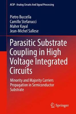
Parasitic Substrate Coupling in High Voltage Integrated Circuits
by Pietro Buccella, Camillo Stefanucci, Maher Kayal, and Jean-Michel Sallese
This book introduces a new approach to model and predict substrate parasitic failures in integrated circuits with standard circuit design tools.
The injection of majority and minority carriers in the substrate is a recurring problem in smart power ICs containing high voltage, high current switching devices besides sensitive control, protection and signal processing circuits.
The injection of parasitic charges leads to the activation of substrate bipolar transistors. This book explores how these events can be evaluated for a wide range of circuit topologies. To this purpose, new generalized devices implemented in Verilog-A are used to model the substrate with standard circuit simulators. This approach was able to predict for the first time the activation of a latch-up in real circuits through post-layout SPICE simulation analysis.
- Discusses substrate modeling and circuit-level simulation of parasitic bipolar device coupling effects in integrated circuits;
- Includes circuit back-annotation of the parasitic lateral n-p-n and vertical p-n-p bipolar transistors in the substrate;
- Uses Spice for simulation and characterization of parasitic bipolar transistors, latch-up of the parasitic p-n-p-n structure, and electrostatic discharge (ESD) protection devices;
- Offers design guidelines to reduce couplings by adding specific protections.


